Projekt URSO180 RetroModern x80-System
URSO180 is the Project to build an 8-bit-Computer like in the days when we could understand all the inner workings of our computer.
However, URSO180 uses more modern technology in order to make the most out of the 8-bit experience. As an aside, this also strives to take out the nuisances that made life more complicated in the early years of DIY-micro-computing.
Intention
A role-model from the early years was and still is the Altair 8800. The Altair started as the minimal computer. It does put nothing of the abstraction layers of more complicated systems between the user and the inner workings.
The Role Model
The Altair has:
- A minimal 8080 (optionally Z80) processor board
- straight, honest static memory
- NO bootstrap monitor that has to be able to run BUT:
- a hardware-based front panel with switches and LEDs to provide functions for
- examining and modifying memory contents
- start and run machine language programs
- halt and single step program execution
The Pupil
URSO180 will have:
- Hitachi HD64180 Processor
- internally a Z80, providing software-compatibility with the largest 8-bit community, including professional-level systems like CP/M
- 10MHz clock frequency
- a built-in MMU - Memory Management Unit allowing addressing up to 1 MByte of memory
- 2 serielle Ports für Terminal und andere Peripherie
- Lagerort: PUCONBOX008204 - Reihe --- - Fach ---
- 1 MByte static RAM
- built from 2 512Kx8bit modules of type SYS8512FKXLI
- gekauft bei eBay
20150103 - eBay - electromyme - SYS8512FKXLI-85 512Kx8bit SRAM Module - eBay-Artikel 281464167318 eBay Item 281464167318
- SYS8512FKXLI-85 512Kx8-Bit 4Mbit Static RAM SRAM Memory Module DIP-32 85ns 5.5V
- Verkäufer: electromyne
- Data sheet: http://scherer3002.duckdns.org/public/public/Projekte/URSO180/SYS8512FKXLI-85_datasheet.pdf
- Lagerort: PUCONBOX008204 - Reihe --- - Fach ---
- up to 512 kByte EPROM/FlashROM (SST Flash-Rom 39SF040 - Lagerort: PUCONBOX006008 - Reihe 005 - Fach ---) for
- Bootloader
- Monitor
- ROM-Disk für CP/M
- ... etc ...
- a front panel like that of the Altair
- shall have the same functionality like that of the Altair
- BUT: Logic in an FPGA
- AND: operation not only by switches and LEDs but by additional logic
- ADDITIONALLY: providing for sort of a Console Processor , bringing more comfort like:
- more comfortable means as Hex-Keyboard and Dot-Matrix-Display
- upload / download interfaces to PC
- automating boot-load-procedures
- storage adapter to SD-cards and USB
Additional Inspiration and Input
When scouring the Web for more detailed information about Z80- and Altair-look-alike-Computers, I found to my delight that I'm by no means the only crazy nerd to build such a thing!
There are a number of people having done extremely thorough work and published it too:
- Ben Ryves built his Z80-Computer Mark 2 with really clever hardware, even including Video output and PS/2 keyboard support. The Mark 2 does not have a front panel with switches and Blinkenlights but sort of a console processor allowing the Z80 to start from scratch without needing (EP)ROM code, similar to the intentions of URSO180
- Grant Searle has a number of simple 8-bit computer designs including some with FPGAs and even completely FPGA-based models.
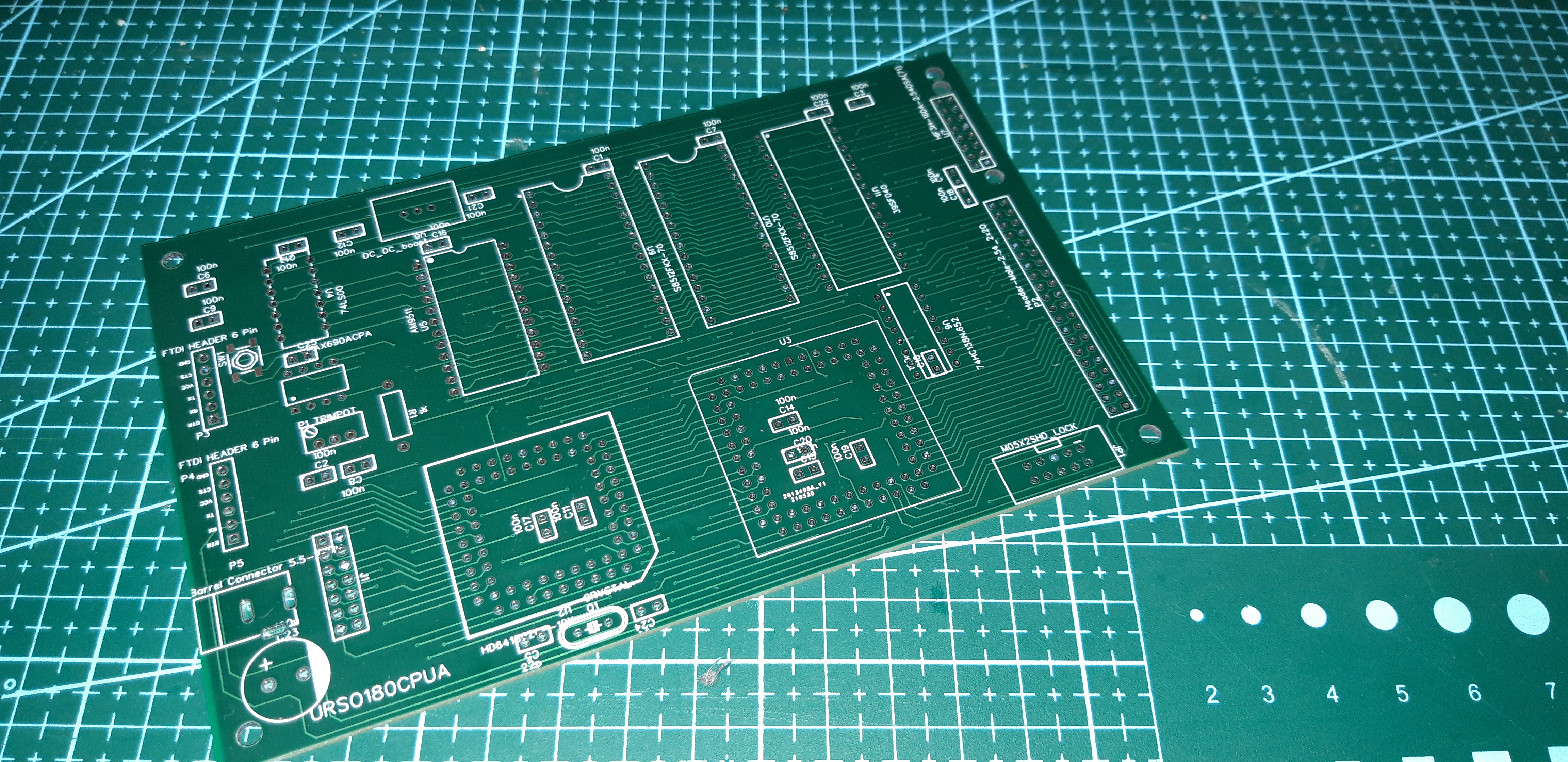
The Hardware
I chose to check out EasyEDA to develop the schematics and possibly even a PCB for the URSO180.
The URSO180 Page is at https://easyeda.com/scherer3002/URSO180-XXwWUgecx.

CPU
The URSO180's CPU is a member of the Hitachi HD64180 family, a HD64180ZCP10X. This specific chip type has the specific parameters:
- 1MiB CPU-addressable memory using a 20-bit address bus
- up to 10MHz internal clock (φ), URSO180 uses a 18.432MHz crystal to generate the clock, resulting in 7.216 MHz internal clock and suiting baud rates on the ACIA channels.
The CPU has internal dual asynchronous serial peripherals. The data signals of both are exposed to the outside world by a 6-pin female header each. These connectors are compatible with most TTL-level FT232 USB-serial bridges. One of these can therefore simply be plugged in the respective female header.
Memory
URSO180 has 1.5 MiB of memory:
- 2 x 512 KiB static CMOS-RAM
- 1 x 512 KiB Flash-ROM 39SF040
The CPU can address 1 MiB directly, the address decoder in the glue logic controls, which of the 3 512KiB physical memory segments is selected in the lower and higher 512KiB segment of the CPU-address space
Glue Logic
The Glue Logic combines most of the remaining logic functions in one component:
- address decoder to produce chip select signals for the 2 RAM-chips and 1 ROM-chip from the 20bit address bus
- additional memeory management logic to select between RAM and ROM in the lower 512 kByte of the address space
- interface I/O port(s) to and from console controller
- Clock divider for the FPU to generate 2 MHz from the 8MHz phi Clock from the processor
Additionally, there are a handful of chips providing specialized functions:
- a MAX690 for generating power-on reset and a watchdog-function.
- a 3-to-8 decoder (74HC138) providing chip-selects for 8 I/O components each occupying 2 I/O-addresses in the 64180's I/O-space
- 2 of these are used on the board:
- the CH376 storage USBhost controller at I/O address 0xF0 and 0xF1
- the AM9511 floating point unit (FPU) at I/O address 0xF2 and 0xF3
- the other 6 (nIOCSF4..nIOCSFE) are output to the expansion connector (P2) to be used in combination with
- data bus D0..D7
- nWR ... write enable
- nRD ... read enable
- 2 of these are used on the board:
- a 74HC00 4 x 2-input NAND gate to invert control signals and select the I/O decoder
The glue Logic core component comes in 2 variants:
Version A: Altera MAX7000S CPLD Glue Logic
This variant uses a EPM7064 CPLD for the Glue Logic functions. This is a rather old CPLD (no FPGA) with rather low function density
Unfortunately, there are no bigger CPLDs or FPGAs operable at 5V Supply, so this has to do for now.
Version B: PSoC as GlueLogic
After design of the URSO180CPUA I started having second thoughts about my decision of part for the glue logic:
- the EPM7064 part is rather "mature" and may go out of production soon
- the logic capacity is low in comparison with more modern parts being this only being a CPLD and not a more veratile FPGA.
This resulted in me not(yet) being able to fit all logic I originally intended into it
On the other hand, modern parts are all 3.3V and therefore not compatible with my 5V-logic HD64180.
In pondering this dilemma, I searched the interwebs for 5V-Logic FPGAs. It should not come as a surprise I came up empty handed as for a 5V-FPGA, BUT I stumbled across an article from a guy who was trying exactly the crazy endevaour I am working on with the URSO180 (so it's not only me being such a retro-nerd ...): 5V Logic on a Z80 Retrocomputer
The project uses a Cypress PSoC 5 chip which is a special type of microcontroller in 2 ways:
- In addition to the RAM, ROM and peripherals of a normal microcontroller it contains an FPGA fabric that can be programmed to emulate a hardware circuit with up to 80MHz processing frequency
- to put the icing on the retro-cake the chip has selectable I/O supply voltage which can range between 2V and 5.5V
So, if using a PSoC-5 chip in the place of the EPM7064 would not only delivers a (hopefully) powerful and versatile enough programmable logic array for the glue logic but also incorporates the (ARM-based 32bit-) microcontroller for providing the console functionality for URSO180.
Furthermore, I happen to have 2 SparkFun FreeSoc-2 boards that I have bought on a whim already some time ago with which I could experiment and develop a Version B of the URSO180-CPU board.
Will continue this road after I've been able to bring the Version A into operation ...
Serial Interfaces
The HD64180 has 3 serial ports, 2 of them can be used in the common UART mode.
The URSO180 tries to provide 2 5/6-pin headers where standard FT232-based USB-serial-adapters can be plugged into. Therefore I tried to determine the most common pinout that allows to plug the USB-serial modules to the edge of the URSO180-board. In the following table there are a number of pinouts to be compared side-by-side
The examples are:
| Number | Image | Link |
|---|---|---|
| 1 | 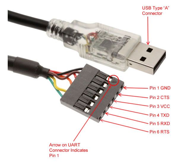 |
Cable |
| 2 | 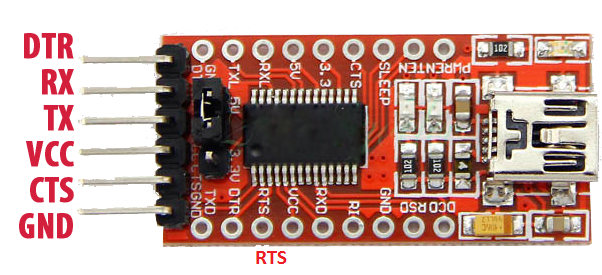 |
Board |
The pinouts are:
| Pin Number | Pinout 1 Function |
Pinout 2 Function |
Pinout 3 Function |
|---|---|---|---|
| 1 | GND | GND | |
| 2 | CTS | CTS | |
| 3 | VCC | VCC | |
| 4 | TXD | TXD | |
| 5 | RXD | RXD | |
| 6 | RTS | DTR |
The Pin Functions are:
(ANN: The Names of the Adapter-Pins are according to the RS-232 / ITU V.24 Specification, the adapter is in the DTE (Data Terminal Equipment) Role, TXD, DTR, RTS are outputs from the adapter, RXD, DSR, CTS, DCD are inputs
| Function Name | Direction | Description |
|---|---|---|
| GND | Adapter -> URSO180 | Ground, common reference for signals and supply voltage |
| CTS | URSO180 -> Adapter | Clear To Send |
| VCC | Adapter -> URSO180 | Supply Voltage Output, taken from USB |
| TXD | Adapter -> URSO180 | Transmit Data |
| RXD | URSO180 -> Adapter | Receive Data |
| CTS | Adapter -> URSO180 | Clear To Send |
Parts
| ID | Name | Designator | Footprint | Quantity | Manufacturer Part | Manufacturer | Supplier | Supplier Part | Price | LCSC Assembly | JLCPCB Part Class |
|---|---|---|---|---|---|---|---|---|---|---|---|
| 1 | 22p | C5,C24 | C1 | 2 | ? | ||||||
| 2 | 100n | C1,C2,C3,C4,C6, C7,C8,C9,C10,C11,C12, C13,C14,C15,C16,C17,C18, C19,C20,C21,C22,C25 | C1 | 22 | ? | ||||||
| 3 | 100u | C23 | CAP-D12.5 - 5.0 | 1 | |||||||
| 4 | Header-Female-2.54_2x7 | J1 | HDR-TH_ 14P-P2.54-V-R2-C7-S2.54 | 1 | 2.54mm, Double female header | ReliaPro | LCSC | C38844 | 0.1127 | Extended Part | |
| 5 | M05X2SHD_LOCK | JP1 | 2X5-SHROUDED_LOCK | 1 | |||||||
| 6 | TRIMPOT | P1 | TRIMPOT | 1 | |||||||
| 7 | Header-Male-2.54_2x20 | P2 | HDR-20X2/2.54 | 1 | Header-Male-2.54_2x20 | ReliaPro | LCSC | C124383 | 0.2151 | ||
| 8 | FTDI HEADER 6 Pin | P3,P4 | HDR-TH_6P-P2.54-V-F | 2 | Female header 1*6p | BOOMELE | LCSC | C40877 | 0.0684 | Yes | |
| 9 | Barrel Connector 5.5-2.1MM | P5 | DC-005 | 1 | DC-005 5.5-2.0MM | ReliaPro | LCSC | C16214 | 0.0458 | ||
| 10 | CRYSTAL | Q1 | HC49S | 1 | |||||||
| 11 | 1k | R1 | R_AXIAL-0.5 | 1 | |||||||
| 12 | Button-SMD-4x4x1.7 | SW1 | SW-SMD_4P-L5.2-W5.2-P3.70-LS6.5 | 1 | 4*4*1.7Plastic head waterproof, 260G, 0.25mm,SMD | BBJ | LCSC | C71847 | 0.0178 | ||
| 13 | MAX690ACPA | U1 | DIP8 | 1 | |||||||
| 14 | HD64180ZCP-10X | U2 | SOCKET_PLCC68 | 1 | |||||||
| 15 | EPM7064SLC-10_PLCC84 | U3 | PLCC-84_THT-SOCKET | 1 | |||||||
| 16 | 74LS00 | U4 | DIP-14_L20.0-W7.6-P2.54-LS8.0-BL | 1 | |||||||
| 17 | AM9511 | U5 | DIP24_600 | 1 | AM9511 | AMD | eBay | ||||
| 18 | 74HC138N,652 | U6 | DIP16 | 1 | |||||||
| 19 | HIF3H-16DA-2.54DSA(71) | U7 | HDR-TH_16P-P2.54-V-R2-C8-S2.54 | 1 | HIF3H-16DA-2.54DSA(71) | Hirose | LCSC | C324996 | 2.5589 | ||
| 20 | DC_DC_boost | U8 | 3PIN_DC_MOD | 1 | noMfgr | AliExpress | noPartNumber | ||||
| 21 | S8512FKX-70 | U9,U10 | DIP-32_ L40.6-W17.8- P2.54-LS15.2-BL | 2 | |||||||
| 22 | 39SF040 | U11 | DIP32 | 1 |
Power Connector
Power is input into the URSO180CPU using a 5.5/2.1mm barrel connector with center-plus polarity.
Tools
- Z80 Assembler:
- C-Compiler
- http://sdcc.sourceforge.net/ - SmallDevice C-Compiler
x80-Resources
- http://www.gaby.de/ - Gaby Chaudry's treasure trove about everything 8080 / Z80 / CP/M / ...
Project Files
... to be continued ...